- 您现在的位置:买卖IC网 > Sheet目录1210 > DLP-HS-FPGA2 (DLP Design Inc)MODULE USB ADAPTER FOR FT2232H
�� �
�
�Simply� connect� the� DLP-HS-FPGA� to� the� PC� to� initiate� the� loading� of� USB� drivers.� Once� the� USB�
�drivers� are� loaded,� the� DLP-HS-FPGA� is� ready� for� use.� All� commands� are� issued� as� multi-byte�
�command� packets� consisting� of� at� least� two� bytes.�
�You� can� either� utilize� the� Test� Application� available� from� http://www.dlpdesign.com/test.shtml� with�
�the� DLP-HS-FPGA� (as� described� in� Section� 12),� or� you� can� write� your� own� program� in� your� language�
�of� choice.�
�If� you� are� using� the� VCP� drivers,� begin� by� opening� the� COM� port,� and� send� multi-byte� commands� as�
�shown� in� Table� 1� below.� There� is� no� need� to� set� the� baud� rate� because� the� DLP-HS-FPGA� uses� a�
�parallel� interface� between� the� USB� IC� and� the� FPGA.� (The� Ping� Command� can� be� used� to� locate� the�
�correct� COM� port� used� for� communicating� with� the� DLP-HS-FPGA,� or� you� can� look� in� Device�
�Manager� to� see� which� port� was� assigned� by� Windows.)� If� you� are� using� the� D2XX� drivers� as� with� the�
�Test� Application,� no� COM� port� selection� is� necessary.�
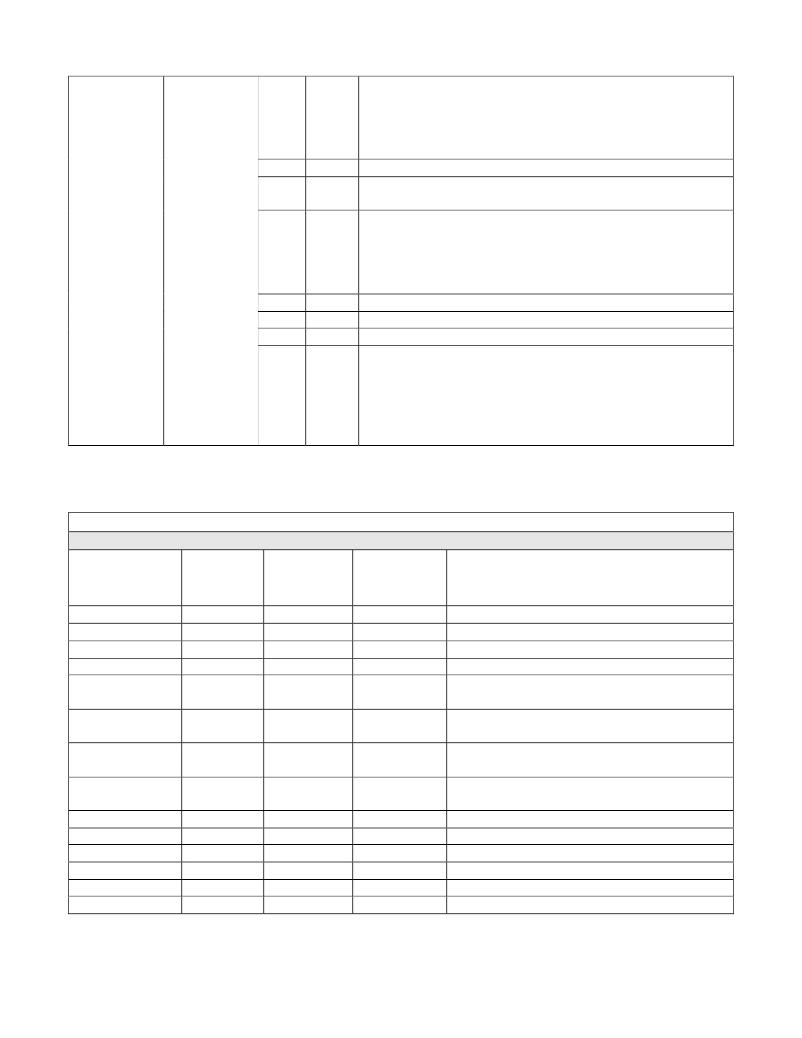
�TABLE� 1�
�Command� Packets�
�Command�
�Hex�
�Packet�
�Description�
�Byte�
�Value�
�Return/Comments�
�Ping�
�Issues� Ping�
�0�
�0x00� Ping� Command� -� 0x56� will� be� returned� indicating� that�
�the� DLP-HS-FPGA� is� found� on� the� selected� port.�
�Read�
�Version/�
�Status�
�Accesses�
�the� internal�
�version/�
�status�
�registers�
�0�
�1�
�0x10� Read� Version/Status� Registers� Command�
�0xnn� Register� Address:� 0xnn� =�
�0x00� =� Board� ID� (0x11� =� Production� PCB)�
�0x01� =� FPGA� Type� ID� :� 0x3A� =� XC3S200A�
�0x4A� =� XC3S400A�
�0x02� =� Design� Version� ID� 1� (Design� Month)�
�0x03� =� Design� Version� ID� 2� (Design� Day)�
�0x04� =� Design� Version� ID� 3� (Design� Year)�
�0x05� =� Design� Version� ID� 4� (Design� Version)�
�0x06� =� DDR2� Status:� 0x00� =� Not� Initialized�
�0x01� =� Initialized�
�Loopback�
�Loopback�
�Compliment�
�Returns� the�
�data� byte�
�received�
�Returns� the�
�compliment�
�of� data� byte�
�0�
�1�
�0�
�1�
�0x20� Loopback� Command�
�0xnn� The� byte� sent� to� the� DLP-HS-FPGA� (0xnn)� will� be�
�returned� back.�
�0x21� Loopback� Compliment� Command�
�0xnn� The� byte� sent� to� the� DLP-HS-FPGA� (0xnn)� will� be�
�complimented� and� returned� back.�
�received�
�Read� Pin�
�Reads� the�
�state� of� one�
�of� the� user�
�I/O� pins�
�0�
�1�
�0x30�
�0x00�
�–�
�0x3E�
�Read� Pin� Command�
�The� user� I/O� pin� numbers� are� described� in� Table� 2.�
�User� I/O� pin� 0xnn� is� read� and� returns:�
�0x00� =� User� I/O� pin� 0xnn� is� low�
�0x01� =� User� I/O� pin� 0xnn� is� high�
�Rev.� 1.7� (May� 2011)�
�10�
�?� DLP� Design,� Inc.�
�发布紧急采购,3分钟左右您将得到回复。
相关PDF资料
DLP-IOR4
MODULE LATCHING-RELAY 4-CH
DLP-TEMP-G
MODULE DATA-ACQUISITION 3-CH
DLP-TXRX-G
MODULE USB-TO-TTL SRL UART CONV
DLP-USB1232H
MODULE USB-TO-UART/FIFO HS 18DIP
DLP-USB232M-G
MODULE USB-TO-TTL SRL UART CONV
DLP-USB232R
MODULE USB-TO-SRL UART 18-DIP
DLP-USB245M-G
MODULE USB-TO-TTL PARL FIFO CONV
DLP-USB245R
MODULE USB-TO-PARL FIFO 18-DIP
相关代理商/技术参数
DLP-HS-FPGA3
功能描述:可编程逻辑 IC 开发工具 USB-to-FPGA Development Module
RoHS:否 制造商:Altera Corporation 产品:Development Kits 类型:FPGA 工具用于评估:5CEFA7F3 接口类型: 工作电源电压:
DLP-HS-FPGA-A
功能描述:FPGA Embedded Module Spartan-3A, XC3S200A FT2232H 66MHz 32MB 制造商:dlp design inc. 系列:FPGA 零件状态:有效 模块/板类型:FPGA,USB ?? 核心处理器:Spartan-3A,XC3S200A 协处理器:FT2232H 速度:66MHz 闪存大小:- RAM 容量:32Mb 连接器类型:USB - B,引脚接头 大小/尺寸:3" x 1.2"(76.2mm x 30.5mm) 工作温度:0°C ~ 70°C 标准包装:1
DLP-IO14
功能描述:数据记录与采集 14-Channel Data-Acq Module
RoHS:否 制造商:Lantronix 描述/功能:Analog device server 显示器类型:None 电流额定值:
DLP-IO16
功能描述:界面模块 USB/Micro Dev Board
RoHS:否 制造商:4D Systems 产品:Serial Converters 通道/端口数量: 数据速率: 接口类型:USB, UART 工作电源电压:3.3 V, 5 V 最大工作温度:
DLP-IO20
功能描述:数据记录与采集 USB-BASED 20-CHANNEL DATA ACQUISITION MOD RoHS:否 制造商:Lantronix 描述/功能:Analog device server 显示器类型:None 电流额定值:
DLP-IO26
功能描述:开发板和工具包 - PIC / DSPIC USB/Micro Dev Board
RoHS:否 制造商:Microchip Technology 产品:Starter Kits 工具用于评估:chipKIT 核心:Uno32 接口类型: 工作电源电压:
DLP-IO8
功能描述:界面模块 USB-BASED 8-CHANL DATA ACQUSITION MODL
RoHS:否 制造商:4D Systems 产品:Serial Converters 通道/端口数量: 数据速率: 接口类型:USB, UART 工作电源电压:3.3 V, 5 V 最大工作温度:
DLP-IO8-G
功能描述:数据记录与采集 USB-BASED 8-CHANL DATA ACQUSITION MODL RoHS:否 制造商:Lantronix 描述/功能:Analog device server 显示器类型:None 电流额定值: